Demystifying Sequential Circuits: An In-Depth Exploration
Published on 12th Aug, 2023
20 min read
Logic Circuits
Circuit Design
Logic Gates
Digital Systems
Welcome to a captivating exploration of sequential logic circuits, the backbone of modern digital electronics. These circuits form the heart of countless electronic devices and systems, enabling everything from smartphones to spacecraft to function seamlessly. In this blog, we'll unravel the intricacies of sequential logic circuits, diving deep into their functioning, applications, and importance in the realm of technology. Prepare to journey through the fascinating world where binary states, clock signals, and logic gates intertwine to create the foundation of our digital age.
What is a Sequential Circuit?
Sequential logic is a type of logic circuit in automata theory. Its output relies on both the current value of input signals and the sequence of past inputs, also known as the input history. This is different from combinational logic where the output only depends on the current input. Sequential logic includes a state or memory, while combinational logic does not.
Block Diagram of Sequential Circuit
In the sequential circuit block diagram shown above, there are 3 Inputs labelled as X1, X2, and X3, and 3 Outputs labelled as Z1, Z2, and Z3. These are connected to a combinational circuit, which is also equipped with 3 Memory Units labelled as "Memory". The outputs from the previous action are stored in the memory units and then passed back to the circuit as Inputs.
A synchronous circuit relies on a clock or clock generator to produce a repetitive sequence of pulses known as the clock signal. This signal is then sent to each memory element in the circuit. The primary memory element used in synchronous logic is known as a flip-flop. In this type of circuit, the output of each flip-flop will only change when triggered by the clock pulse. As a result, any changes made to the logic signals throughout the circuit will occur simultaneously at regular intervals, which are synchronized by the clock. Nearly all sequential logic today is clocked or synchronous logic.
The circuit's state is determined by the binary data stored in its flip-flops at any given time. In a synchronous circuit, the state only changes during clock pulses. The next state is determined by the current state and input signals when the clock pulse occurs during each cycle.
Synchronous logic has a simple advantage - the logic gates that manipulate data take a finite amount of time to react to input changes, known as propagation delay. For a stable and reliable circuit, the clock pulse interval must be long enough for the logic gates to respond to changes and settle their outputs to stable logic values before the next pulse. Provided this condition is met, disregarding other details, the circuit's maximum operating speed is determined.
There are two primary drawbacks to synchronous logic:
In a circuit, the maximum clock rate is determined by the slowest logical calculation, referred to as the critical path. All logical calculations, whether simple or complex, must be completed within a single clock cycle. As a result, logic paths that finish their calculations quickly have idle time while waiting for the next clock pulse. Therefore, synchronous logic can be slower than asynchronous logic. To improve the speed of synchronous circuits, a technique called pipelining can be used. This involves breaking down complex operations into simple ones that can be completed in successive clock cycles. The technique is commonly used in microprocessor design and can enhance the performance of modern processors.
To ensure the proper functioning of the circuit, the clock signal should be transmitted to all flip-flops. As this signal is often high-frequency, it utilizes a significant amount of power and generates heat, even in unused flip-flops. In battery-operated devices, it's necessary to implement extra hardware and software to decrease the clock speed or turn off the clock temporarily to preserve battery life when the device is not in use.
Asynchronous Sequential Circuit
Asynchronous sequential logic, also known as clockless or self-timed logic, operates independently of a clock signal. This means that the circuit's outputs change directly in response to changes in inputs. The main advantage of using asynchronous logic is that it can be faster than synchronous logic, as it doesn't have to wait for a clock signal to process inputs. This means that the speed of the device is potentially limited only by the propagation delays of the logic gates used.
In various synchronous systems where speed is essential, asynchronous sequential circuits are utilized in specific critical components, such as digital signal processing circuits or microprocessors. The creation of asynchronous logic involves distinct mathematical models and techniques compared to synchronous logic and is currently an area of active research.
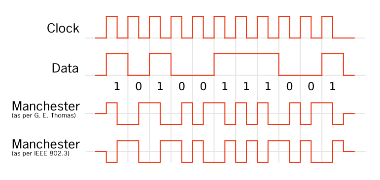
Clock Signal
In the field of electronics, specifically in synchronous digital circuits, a clock signal (also referred to as a logic beat in the past) is an electronic signal that alternates between high and low states at a consistent frequency. This signal serves as a metronome for synchronizing digital circuits. In synchronous logic circuits, which are the most commonly used type of digital circuit, the clock signal is applied to all storage devices, flip-flops, and latches. This causes them to change their state at the same time, thus avoiding race conditions.
An electronic oscillator, known as a clock generator, creates a clock signal. The typical form of this signal is a square wave with a duty cycle of 50%. Circuits that use this signal for synchronization can activate on either the rising edge, falling edge, or both the rising and falling edges of the clock cycle in the case of a double data rate.
Latch & Flip-flop
Flip-flops and latches are circuits found in electronics that have two stable states, allowing them to store state information. These circuits are known as bistable multivibrators and can be controlled to change their state by signals applied to one or more control inputs. Their output state, along with its logical complement, can be obtained. They are the basic storage elements in sequential logic and are essential building blocks of digital electronics systems. These systems are widely used in computers, communications, and many other types of systems.
You can design it using Latches along with a clock.
You can design it using Logic gates.
Sensitivity
A flip-flop is sensitive to the applied input and the clock signal.
Latches are sensitive to the applied input signal- only when enabled.
Operating Speed
It has a slow operating speed.
It has a comparatively fast operating speed.
Classification
You can classify a flip-flop into a synchronous or asynchronous flip-flop.
A user cannot classify the Latch this way.
Working
Flip-Flops work using the binary input and the clock signal.
Latches operate only using binary inputs.
Power Requirement
It requires more power.
It requires comparatively less power.
Analysis of Circuit
It is quite easy to perform circuit analysis.
Analyzing the circuit is quite complex.
Type of Operation Performed
Flip-flop performs Synchronous operations.
Latch performs Asynchronous operations.
Robustness
Flip-flops are comparatively more robust.
Latches are comparatively less robust.
Dependency of Operation
The operation relies on the present and past input bits along with the past output and clock pulses.
The operation depends on the present and past input along with the past output binary values.
Usage as a Register
A flip-flop is capable of working as a register as it contains clock signals in its input.
A latch cannot serve as a register as the register requires further advanced electronic circuits (EC). Time also plays an essential role here.
Types
J-K, S-R, D, and T Flip-flops.
J-K, S-R, D, and T Latches.
Area Required
It requires more area.
It requires comparatively less area.
Uses
They constitute the building blocks of many sequential circuits such as counters.
Users can utilize these for designing sequential circuits. But they are still not generally preferred.
Input and Output
A flip-flop checks the inputs. It only changes the output at times defined by any control signal like the clock signal.
The latch responds to the changes in inputs continuously as soon as it checks the inputs.
Synchronicity
A flip-flop is synchronous. It works based on the clock signal.
A latch is asynchronous. It does not work based on the time signal.
Faults
Flip-Flops stay protected against any fault.
The latches are responsive to any occurring faults on the enable pin.
There are four common types of flip-flops and latches, namely SR (set-reset), D (data or delay), T (toggle), and JK. The behaviour of a specific type can be explained using its characteristic equation, which determines the next output, Qnext, after the next clock pulse based on the input signal(s) and/or the current output Q.
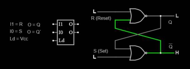
Simple set-reset latches (S-R Latches)
One of the most basic latches when using static gates as building blocks is the SR latch. The letters "S" and "R" stand for "set" and "reset" respectively. It is made up of two cross-coupled NOR or NAND logic gates. The output marked "Q" displays the stored bit.
While the R and S inputs are both low, feedback maintains the Q and Q' outputs in a constant state, with Q' the complement of Q. If S (Set) is pulsed high while R (Reset) is held low, then the Q output is forced high, and stays high when S returns to low; similarly, if R is pulsed high while S is held low, then the Q output is forced low and stays low when R returns to low.
Experience the NOR-Based S-R Latch through an online simulation. Click here to begin.
Note: The symbol "?" indicates that either 0 or 1 is a valid value and is not of significance.
When both NOR gates output zeros, the combination of R = S = 1 is known as a restricted combination or a forbidden state. This combination violates the logical equation Q = not Q', making it unsuitable for circuits where both inputs may decrease simultaneously. This could result in a transition from restricted to keep, causing the output to lock at either 1 or 0, depending on the propagation time relations between the gates, which is known as a race condition.
In order to bypass the limited combination, gates can be added to the inputs to convert (S, R) = (1, 1) to one of the unrestricted combinations. Some examples of these combinations include:
Q = 1 (1, 0) – referred to as an S (dominated)-latch
Q = 0 (0, 1) – referred to as an R (dominated)-latch
While the R and S inputs are both high, feedback maintains the Q and Q' outputs in a constant state, with Q' the complement of Q. If S' (Set) is pulsed high while R' (Reset) is held low, then the Q output is forced low, and stays low when S' returns to low; similarly, if R' is pulsed high while S' is held low, then the Q output is forced high and stays low when R returns to low.
Experience the NAND-Based S'-R' Latch through an online simulation. Click here to begin.
When teaching about SR latches, beginners often find it difficult to grasp the concept of a pair of cross-coupled components such as transistors, gates, or tubes. To make it simpler for learning purposes, it's better to represent the latch as a single feedback loop instead of cross-coupling. Here, we have an SR latch constructed using an AND gate with one inverted input and an OR gate. It's worth noting that the inverter is not essential for the latch functionality but is only used to make both inputs High-active.
Experience the AND-OR-Based S-R Latch through an online simulation. Click here to begin.
S
R
Action
0
0
No change; random initial
1
0
Q = 1
?
1
Q = 0
Please note that the SR AND-OR latch has a distinct advantage in that the values of S = 1 and R = 1 are well-defined. In the above version of the latch, the R signal takes priority over the S signal. However, if you require priority for S over R, you can achieve this by connecting the output Q to the OR gate's output instead of the AND gate's output.
S-R Flip-flop
The S-R flip-flop is a commonly utilized circuit component, referred to as either a "set-reset" flip-flop.
During a specific part of the clock cycle, like the rising edge, the S-R flip-flop preserves the value of the S-input and makes it the Q output. The output Q remains constant at other times. Essentially, the S-R flip-flop functions as a memory cell, a zero-order hold, or a delay line.
The D flip-flop is a popular component used in various applications and is alternatively referred to as a "data" or "delay" flip-flop. Its primary function is to capture the value of the D-input during a specific point of the clock cycle, like the rising edge of the clock. This captured value then becomes the Q output, which remains unchanged during other times. The D flip-flop can also be perceived as a memory cell, a zero-order hold, or a delay line.
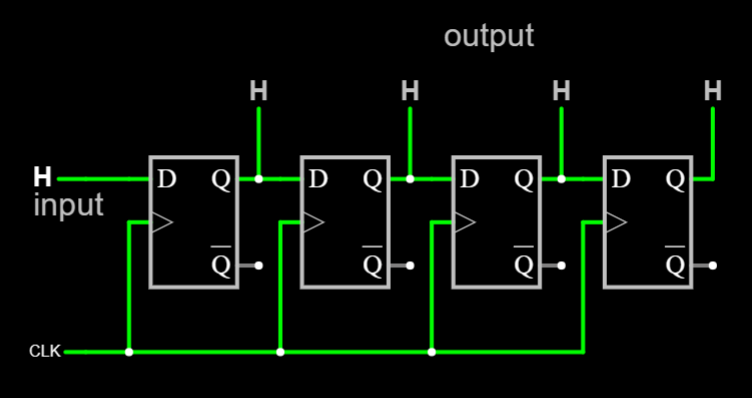
Importance of D Flip-flop in Shift Registors
Flip-flops are crucial components of electronic devices, and they serve as the foundation for shift registers. The D flip-flop has an advantage over the D-type "transparent latch" because it captures the signal on the D input pin as soon as it's clocked. Any further changes on the D input are ignored until the next clock event. However, some flip-flops do have a "reset" signal input, which resets Q to zero. This reset may be either asynchronous or synchronous with the clock.
This circuit shifts the register contents to the right by one bit position during each active transition of the clock. The input X is then shifted into the leftmost bit position.
J-K Flip-flop
The JK flip-flop is an extension of the SR flip-flop, with J meaning "Set" and K meaning "Reset." The condition where J and K are both 1 is interpreted as a "flip" or toggle command. If J is 1 and K is 0, it sets the flip-flop. If J is 0 and K is 1, it resets the flip-flop. If J and K are both 1, it toggles the flip-flop and changes its output to the opposite of its current value. If J and K are both 0, the current state is maintained. To make a D flip-flop, set K to the opposite of J (J will be the input for D). To make a T flip-flop, set K to J. Therefore, the JK flip-flop is a universal flip-flop because it can function as an SR flip-flop, D flip-flop, or T flip-flop.
The characteristic equation of the JK flip-flop is: Qnext = JQ' + K'Q
When the T input is set to high, the T flip-flop will toggle its state each time the clock input is strobed. On the other hand, if the T input is low, the flip-flop will retain its previous value. This behaviour can be explained by the characteristic equation: Qnext = T⊕Q = TQ' + T'Q
If T is set to high, the toggle flip-flop will divide the clock frequency by two. This means that if the clock frequency is 4 MHz, the output frequency from the flip-flop will be 2 MHz. This feature is commonly used in digital counters. It is also possible to create a T flip-flop using a JK flip-flop (by connecting J and K pins together to act as T) or using a D flip-flop (by driving the D input with the T input XOR Qprevious).
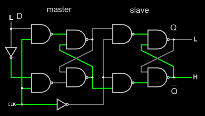
Master-Slave Flip-flop
The Master-Slave Flip-Flop is a combination of two JK flip-flops connected in a series. One flip-flop is the "master" and the other is the "slave". The output from the master flip-flop is connected to the inputs of the slave flip-flop, and the output of the slave flip-flop is fed back to the inputs of the master flip-flop. Additionally, an inverter is included in the circuit. The inverter is connected to the clock pulse so that the inverted clock pulse is given to the slave flip-flop. In other words, if the clock pulse is 0 for the master flip-flop, then it's 1 for the slave flip-flop, and if the clock pulse is 1 for the master flip-flop, then it's 0 for the slave flip-flop.
Experience the AND-OR-Based S-R Latch through an online simulation. Click here to begin.